

A hundred and thirty-two small machines
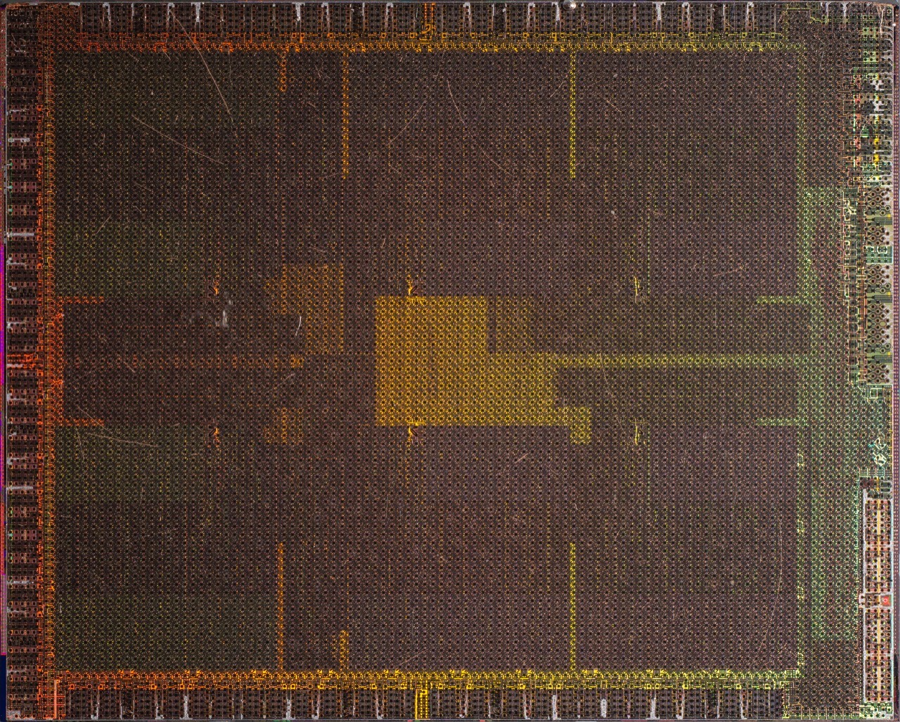
Count the independent compute units on each chip and the two designs separate on the first line. A TPU has at most two TensorCores. An H100 has 132 streaming multiprocessorsOne of a GPU’s many cores; each keeps many warps resident and switches among them to hide memory latency.taught in /l/tpu → and a B200 measures at 148 (a microbenchmark figure; NVIDIA publishes no count), each one independent of the others, so a GPU can run hundreds of separate tasks at once. Any single SM is much weaker than a TPU TensorCore. The chip as a whole is much more flexible.
That independence has a ceiling, and the ceiling is the L2 cache. All 132 SMs share roughly 50 MB of it, which means units that are architecturally independent still end up coordinating in practice, because they are competing for the same lines. You change a memory access pattern in one kernel and a different kernel's throughput moves. The scaling book's phrasing for this is action at a distance, and it is the reason GPU programmers talk about cache behavior the way TPU programmers talk about block sizes.
schematic drawn after NVIDIA H100 whitepaper Figure 6 (full GH100 die); block proportions indicative, counts as published
Inside one SM
Open an SM and you find four identical quadrants, which NVIDIA calls subpartitions. Each one holds a Tensor Core, a warp32 GPU threads scheduled as one unit; the GPU hides latency by switching among resident warps rather than by pipelining a scratchpad.taught in /l/tpu → scheduler, 32 fp32 CUDA cores that all execute the same instruction in a given cycle, and its own register file of 16,384 32-bit words. Four register files put 256 kB of register memory in every SM. Next to them, shared across all four subpartitions, sits 256 kB of SMEMScalar memory: lengths, flags, and indices live here, feeding control flow without ever entering the vector datapath.taught in /l/tpu →: an on-chip cache you can either leave to the hardware or drive yourself as shared memory.
Nearly all the arithmetic lives in the Tensor Cores. An H100 does 990 bf16 TFLOPs/s through them against 66 TFLOPs/s from the CUDA cores, a factor of about 15. Divide that 990 by 132 SMs, 4 subpartitions, and the 1.76 GHz the scaling book uses for the arithmetic, and each Tensor Core is doing roughly 1024 bf16 FLOPs per cycle, about the work of an 8x8x8 matmul. NVIDIA publishes almost nothing about the internals, so read that as an inference from the published totals rather than a datasheet line. The same division on a B200 lands near 2048.
Blackwell grew the Tensor Core past what the older memories could feed it. In Ampere a single warp32 GPU threads scheduled as one unit; the GPU hides latency by switching among resident warps rather than by pipelining a scratchpad.taught in /l/tpu → could feed the unit, in Hopper it takes a full warpgroup, and in Blackwell it is fed from two SMs at once; by then the accumulator no longer fits in registers or SMEM. So a B200 adds a separate 256 kB of Tensor Memory per SM to hold the arguments.
SIMT, and the divergence a TPU cannot have
The 32 CUDA cores in a subpartition execute the same instruction each cycle, which is exactly what the ALUs in a TPU's VPUThe vector unit for elementwise work, organized as (8, 128) lanes; the origin of the tiling lattice every layer above obeys.taught in /l/tpu → do. The difference sits one level up. Each CUDA core, called a thread in CUDA's vocabulary, has its own instruction pointer, and a warp32 GPU threads scheduled as one unit; the GPU hides latency by switching among resident warps rather than by pipelining a scratchpad.taught in /l/tpu → is the group of 32 threads that one warp scheduler dispatches together. NVIDIA calls the model SIMT, single instruction multiple threads, against the TPU's SIMD.
So you can write a branch whose two sides are taken by different threads of the same warp. The hardware will not refuse it. It runs both sides and masks off the cores that should not be executing the current one, so a warp32 GPU threads scheduled as one unit; the GPU hides latency by switching among resident warps rather than by pipelining a scratchpad.taught in /l/tpu → that diverges pays for both branches. Nothing on a TPU can do this: the VPUThe vector unit for elementwise work, organized as (8, 128) lanes; the origin of the tiling lattice every layer above obeys.taught in /l/tpu → has one instruction pointer for the whole unit and no per-lane state to diverge with. Divergence is not a TPU hazard you learn to avoid, it is a category that does not exist there. Threads are also freer about memory, reaching individual values in shared memory and keeping per-thread state, where the VPU only operates on contiguous blocks.
Scheduling is the second freedom. An SM can hold up to 64 resident warps32 GPU threads scheduled as one unit; the GPU hides latency by switching among resident warps rather than by pipelining a scratchpad.taught in /l/tpu → and the warp scheduler switches between them to hide memory loads, roughly the way a multi-threaded CPU does. Registers are what stop you. A thread can address at most 256 registers, and at that ceiling only 8 warps fit at once in an SM's 256 kB register file. TPUs are single threaded by comparison, which is why their loads have to be pipelined by the compiler instead of covered by a scheduler at runtime.
The memory ladder
Below registers and SMEMScalar memory: lengths, flags, and indices live here, feeding control flow without ever entering the vector datapath.taught in /l/tpu → sits the L2, about 50 MB on an H100. It is physically split in two, so half the SMs reach 25 MB a piece, with a link between the halves at lower bandwidth. NVIDIA does not publish its bandwidth; measurements put it near 5.5 TB/s, roughly 1.6x HBMThe chip’s main memory: large, far, and the resource memory-bound ops spend. 8.2e11 bytes per second on v5e, 1.6e12 on v6e.taught in /l/tpu → bandwidth, and because it is full-duplex the effective bidirectional figure is closer to 3x. It is the nearest thing the GPU has to VMEMThe TPU’s software-managed vector scratchpad, about 128 MiB. Blocks must be staged here before compute touches them; what is resident is what your schedule staged.taught in /l/tpu → by size. It is much slower, and unlike VMEM you do not control it.
Under everything is HBMThe chip’s main memory: large, far, and the resource memory-bound ops spend. 8.2e11 bytes per second on v5e, 1.6e12 on v6e.taught in /l/tpu →: 80 GB at 3.4e12 bytes/s on an H100, 192 GB at 8.0e12 bytes/s on a B200. Those two numbers are the ones you divide against FLOPs to get a ridgeThe FLOP-per-byte ratio where an op flips from memory-bound to compute-bound: about 240 on v5e, about 575 on v6e.taught in /l/tpu →, the same arithmetic stage 0 does for a v5e, and the reason the whole memory ladder above exists is to keep traffic off that bottom rung.
| level | H100 | B200 |
|---|---|---|
| SMs / chip | 132 | 148, measured |
| registers / SM | 256 kB | 256 kB |
| SMEM / SM | 256 kB | 256 kB |
| TMEM / SM | none | 256 kB |
| L2 / chip | 50 MB | 126 MB |
| HBM / chip | 80 GB | 192 GB |
| HBM bandwidth | 3.4e12 B/s | 8.0e12 B/s |
Two things named Tensor Core
One term does two different jobs across the two vendors, and it causes real confusion when you read both sets of docs in a week. On a TPU, the TensorCore is the umbrella unit: it contains the MXUThe systolic matmul array: 128x128 on v5e, 256x256 on v6e. Matmuls only; everything else is the VPU’s job.taught in /l/tpu →, the VPUThe vector unit for elementwise work, organized as (8, 128) lanes; the origin of the tiling lattice every layer above obeys.taught in /l/tpu →, and the machinery around them. On a GPU, the Tensor Core is only the matrix multiplication sub-unit inside a subpartition, one of four in an SM. The unit that plays the TPU TensorCore's role on a GPU is the SM itself.
A TPU TensorCore contains an MXU. A GPU Tensor Core is one.
Hold that straight and the rest of the vocabulary lines up cleanly: warp32 GPU threads scheduled as one unit; the GPU hides latency by switching among resident warps rather than by pipelining a scratchpad.taught in /l/tpu → scheduler against VPUThe vector unit for elementwise work, organized as (8, 128) lanes; the origin of the tiling lattice every layer above obeys.taught in /l/tpu →, CUDA core against VPU ALU, SMEMScalar memory: lengths, flags, and indices live here, feeding control flow without ever entering the vector datapath.taught in /l/tpu → against VMEMThe TPU’s software-managed vector scratchpad, about 128 MiB. Blocks must be staged here before compute touches them; what is resident is what your schedule staged.taught in /l/tpu →, HBMThe chip’s main memory: large, far, and the resource memory-bound ops spend. 8.2e11 bytes per second on v5e, 1.6e12 on v6e.taught in /l/tpu → against HBM. The two-machines lesson later in this stage puts the counts side by side, which is where the two designs stop looking alike.
Check yourself
01 What is the ceiling on SM independence?
The shared L2: all the SMs compete for the same lines, so one kernel's access pattern moves another kernel's throughput.
02 What stops you keeping 64 warps resident on an SM?
Registers: at 256 registers per thread only 8 warps fit the 256 kB register file, so occupancy falls as register pressure rises.
Readings
- Scaling book · How to think about GPUs ↗ every number in this lesson comes from here; start at the SM section
- SemiAnalysis · the Tensor Core from Volta to Blackwell ↗ how the matmul unit grew until it needed a memory of its own
- Cornell · understanding GPU architecture ↗ the slower walk through SMs, warps, and occupancy
- How to optimize a CUDA matmul ↗ the same hierarchy seen from inside a kernel, step by step